Our founding mission is to make computer science and digital electronics accessible to students, hobbyists, and curious museum-goers around the world. We have since branched out into consumer products and usability design, including IoT, toys, electronic art, jewelry, educational, and personal electronics. (Contact us at  )
)
Happy 52nd Anniversary 4004! (b: November 15, 1971)
Congratulations to Klaus Scheffler and Lajos Kintli
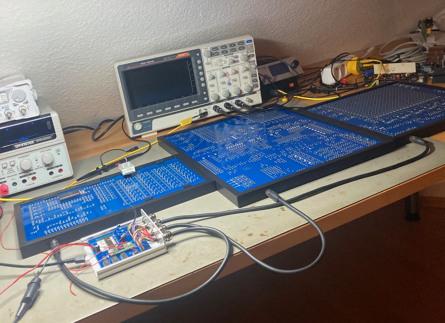
To celebrate the 52nd Anniversary of Intel’s November 15, 1971 product launch of the now-historic 4004 microprocessor, Swiss physicist, Klaus Scheffler, in a world’s first, built a complete 4-bit computer based on Intel’s original 4004 schematics using nearly 4,000 discrete SMD transistors on three giant printed circuit boards. He proved his computer works stand-alone by running an algorithm that computes the first 16 digits of Pi. This achievement was an international collaboration with Hungarian mathematician, Lajos Kintli, who worked with Scheffler from afar to debug the printed circuit “microprocessor,” by writing assembly-language algorithms for the 4004, “board bring-up” test software running on a Teensy, and Kintli’s indispensable circuit analyzer and verification software that made it possible for Sheffler to build and debug his fledgeling, printed circuit 4004 incrementally, comparing it against “oscilloscope traces” from Kintli’s known-working simulation of the entire 4004-family chip-set. But Scheffler did not stop there. After he got his transistor 4004 working, he went on to build a transistor 4002 RAM and a hybrid ROM+I/O board to create a complete, stand-alone, 4-bit computer. This project is a testament that a “big hack” (the good kind) can be accomplished by a small team of dedicated hobbyists or even solo, working just a few hours a week, yet persisting for months despite the inevitable technical challenges.
March 4, 2025 update: Additional work by Sheffler and Kintli have finally yielded performance results that exceed the original 4004's 750kHz. They can now run the discrete transistor 4004 at 1,070 kHz (1.4x faster than the original).

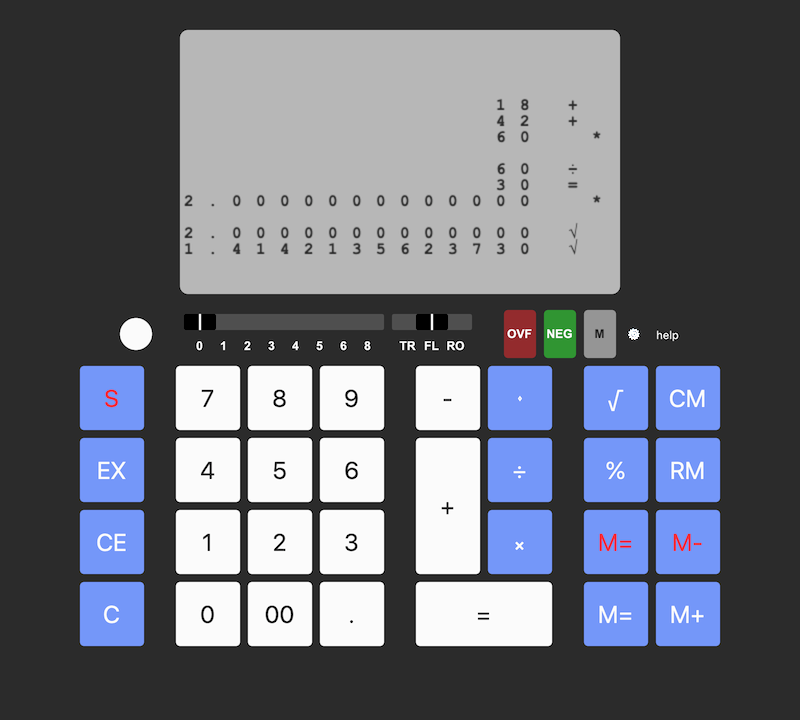
Check out Chen Steenvoorden's Busicom 141-PF Printing Calculator Simulator implemented in WebAssembly.
Note best: The the 141-PF was a vintage adding machine, so you'll see the digits you typed on "paper" only after you press an operator button like "plus."
For example: To add 18 and 42, type 1 8 + 4 2 + = (The 2nd + is very important!)
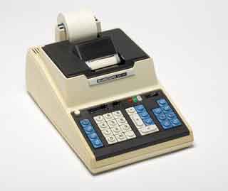
You can read the original (Busicom clone) Operating Instructions at the Internet Archive.

Federico Faggin published his memoirs in Italian and English (February 2021)
The autobiography of this award-winning pioneer of semiconductor technology, designer of the 4004, 8008, 8080, Z80, etc., first published in Italian (as Silicio), now out in English Silicon: From The Invention of the Microprocessor to the New Science of Consciousness
Last year's shout-out went to Erturk Kocalar (November 2020)
...for his line of educational (and open-source) Arduino-compatible "Retroshield" kits that let you play around with real, vintage microprocessors from the comfort of your laptop. He recently released his most ambitious shield yet—you guessed it—the ZIF socketed, preassembled 4004 Retroshield, complete with voltage level-shifters so the -15 volt PMOS 4004 can communicate with the 5 volt CMOS Arduino. I particularly like Erturk's Busicom calculator technical summary, which includes a nice explanation of how the Shinshu Seiki drum printer works.
Want to meet a community of vintage semiconductor engineers we inspired? Visit the Visual 6502 Project and Evil Mad Scientist Laboratories
Want to know more about the "F.F." signature in the corner of the chip? Read the perspective of Federico Faggin, the 4004's silicon designer.
The Exhibit Story
Genesis
Knowing that robotic "pick-and-place" machines were now the standard way of assembling electronics, and made the whole idea practical to produce, I started thinking. What could I build out of this "retro," one-gate-per-chip technology? Some sort of microprocessor seemed like a natural. But modern microprocessors have millions of transistors, so I knew I'd have to keep the project very modest, like restricting the data-path to 4-bits. This meant I'd have to design my own, or... go back in history and build a replica of a commercial micrprocessor. Besides, reproducing a commercial microprocessor, rather than re-inventing my own, would allow me to use existing software and existing manuals, data sheets, wisdom of the ages, etc.
The first microprocessor that came to mind was the Intel 4004. It was not nearly as famous as the 8080, and its 8-bit progeny, but my late step-father, Joe Robb, worked for Intel in the early 1970's, and I still remember when brought home some MCS-4 data sheets. MCS-4 (Microcomputer Set 4) was the name Intel gave to the 4004 chip family for its commercial introduction in November 1971.
In search of the circuit
During this research spree I also learned that the Intel Archives and the Intel Museum were somehow connected. This helped me turn a notion into a plan: I wrote to Tracey Mazur, the curator of the Intel Museum, and Rachel Stewart, Intel's corporate archivist, with a proposition: if you give me access to internal 4004 engineering documents, I will build you a giant, functioning replica of the 4004 suitable for a museum exhibit.
Around the same time I started looking for vintage software to run on the giant 4004 replica. I wrote to Federico Faggin and to Marcian "Ted" Hoff, two of the four co-inventors of the 4004 (I was never able to contact the other inventors, Busicom's Masatoshi Shima or Intel's Stan Mazor). Both Faggin and Hoff wrote back, Faggin with a general offer of advice, and Hoff with software for a 4004-based video game design that Intel pitched to a potential customer.
At this time, I was not optimistic about gaining access to schematics or the mask artwork that was used to create the original 4004 wafers, and so I began devising a "Plan B." I was even starting to wonder if there were any schematics to be found, having read interviews that suggested that no complete logic diagram was ever drawn of the 4004. In consultation with Federico Faggin and MIT's Tom Knight, I mentally prepared myself for reverse-engineering the 4004 "the old-fashioned way," by photographing the metal layer through a microscope, and then etching that top layer away to reveal the polysilicon layer, photographing that, and using enlargements of these photomicrographs to meticulously transcribe every transistor and wire.
A few weeks later I got word from Tracey Mazur that Intel's legal department would allow us access to the 4004 engineering documents, and Rachel Stewart was offering encouraging news about her research.
In late July of 2005 I flew to California to meet with Federico Faggin and Rachel Stewart at the Intel archives. The visit was amazingly brief and nearly a complete success. Faggin picked up three large engineering drawings on vullum, a translucent plastic sheeting, unrolled them one-by-one, and declared within 30 seconds, "Yes. This is all of them." Rachel and I looked at each other approvingly, as Faggin adds, "See here? The drawings are drawn just like the chip layout."
The Calculator connection
Reverse Engineering the schematics
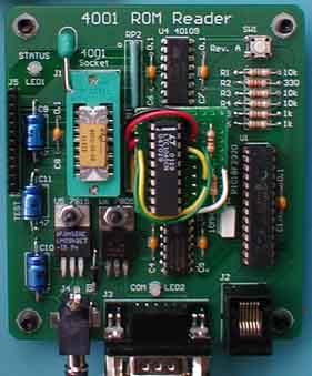
Meanwhile I continued to develop the ROM reader, periodically sending Brian and Barry my results to see if the binary data I was extracting yielded valid 4004 code. After some struggles with the unusual voltage levels used by the 4001 ROMs, we succeeded in extracting a significant fraction of the Busicom software from the ROMs Faggin had found in his basement. The bad news was that there were large strings of zeros in three out of four of the calculator ROMs. We would have to find another source.
Digital Archeology Expedition
After Fred returned to Boston, I immediately sent the ROM contents to Brian and Barry, who used Fred's wiring diagram along with printed circuit board photographs I received from Christian Bassow, a German chip collector. Within a month, they had crafted an instruction-level simulator of the 4004 as well as simulated Busicom hardware, and by January 2006, they had a completely working simulation of the Busicom 141-PF printing calculator.
Verilog simulation of the 4004
Funding and Exhibit design
Letting visitors "look under the hood"
Exhibit Detail and Construction
Out of the vaults and into the world
Concurrently with the exhibit contruction, I started having conversations with Tracey behind the scenes to see if we could get Intel to release the 4004 schematics, mask works, and MCS-4 Users Manual into the public domain. After all, what is the point of keeping historic technology locked up in a vault once its only value is historical? At this writing, Intel has agreed to license these documents for non-commercial use.
Download Stuff Here ( )
)
Updated Busicom 141-PF calculator software, fully commented and documented (Text, Updated 11/17/2009)
Bill Kotaska's Busicom 141-PF replica: Photos, schematics, and narrative — (v2: Updated 11/18/08)
Tim McNerney's Shinshu Seiki Model-102 printer emulator for PIC18F2320
Busicom 141-PF calculator simulator with flowchart (Zip) Documentation
-
Tim McNerney's talk at 35th Anniversary event (13-Dec-2006)
(MP3, 20min 47sec, © 2006 Computer History Museum)
Transcript of talk Lajos Kintli's Intel 4004 netlist/layout analyzer with animated logic simulator with complete MCS-4 masks and schematics (Zip, v2.0: updated 11/15/2018)
Frequently Asked Questions
How can I contact you?
If you want information about our products or services, you are interested in volunteering, or you have an interesting suggestion, contact me, Tim McNerney at 
Are you looking for volunteers, interns, or collaborators?
Yes! We are looking for electrical engineers, computer scientists, and VLSI designers to help us analyze the inner workings of the Intel 4004 hardware down to the transistor level and the Busicom 141-PF calculator software down to the instruction level, and K-12 teachers, professors, writers, graphic designers, information designers, and web technologists to document, illustrate, and explain the elegant beauty of this historic microprocessor system to students, lay people, and future historians.
Do you offer products or services?
The Intel Museum has given us permission to offer our exhibit technology to other museums and institutions, including fully functional 130x scale replicas of the 4004 built using discrete transistors, museum-durable keyboards and slide switches, and video display electronics.
We had planned to offer a limited edition, Busicom 141-PF replica built using vintage 4004-family chips, but we never figured out a good "retro" substitute for the Epsom drum printer. The vintage Intel chips are expensive and in short supply, but if there is sufficient interest in these, or a more affordable replica built using modern chips, yet still running the original Busicom software, we would be happy to revisit this, perhaps as a Kickstarter campaign.
So who were those anonymous "digital archeologists" reported in the Slashdot article?
They were Fred Huettig, Brian Silverman, Barry Silverman, Lajos Kintli, and myself. Sellam Ismail performed the delicate surgery on the archeological artifact that Federico Faggin donated to the Computer History Museum
Is the Intel 4004 really the world's first microprocessor?
Yes and no, but mostly yes. The Intel 4004 is widely considered to be the world's first general-purpose CPU-on-a-chip. But there were pioneers of LSI technology at other companies who also deserve credit for their work. Some had to work in secret and wait for their work to become declassified years later. Intel makes no such bold claims (wishing to avoid more spurious lawsuits), but there is no doubt that the 4004 was the first customer-programmable microprocessor to reach the commercial market. You simply could not buy anything like it before its introduction on November 15, 1971...[Read More about the nuances here.]
The 4004 was manufactured from 1971 to 1986, any idea why it lasted so long?
Short answer: Because it was cheap, elegant, scalable, and required no "glue logic"... [Read more]
Where can I buy individual, vintage chips?
I have seen 4004s and related chips (4001, 4002, 4003, 4008, 4009, 4040, 4201, 4289) for sale on eBay. Search for P4004 (P = plastic package), D4004 (D = brown ceramic), and C4004 (C = white ceramic). The white ceramic packages sell for hundreds of dollars, but the other packages are more affordable. The early grey-on-white ceramic packages are extremely rare.
I bought a 4004 on eBay. Do you think it still works?
All these chips are static sensitive. Only if you (and the seller) handle the chip carefully, just like a memory upgrade to your computer, can you avoid "zapping" it (which would render it inoperative or intermittent). If your chip arrived in anti-static foam (usually black) and wrapped in aluminum foil or anti-static plastic (usually pink), then it may still work, even after 35 years. Right now, the only way to find out if it works for sure is to build an electronics project that uses your 4004.

Intel 4004 35th Anniversary Exhibit Project
Credits
Team Personnel (in alphabetical order)
-
Allen E. Armstrong, mechanical engineering
-
Fred Huettig, netlist extraction software, electrical engineering, FPGA programming
- Lajos Kintli, reverse-engineering, software analysis, commenting, documentation
-
Tim McNerney, conceptual design, project leader, digital design
-
Barry Silverman, reverse-engineering, simulation software
-
Brian Silverman, reverse-engineering, simulation software
Collaborators and advisors
- Federico Faggin, CEO Foveon, 4004 chip designer
- Sellam Ismail, proprietor, Vintage Tech
- Tom Knight, MIT CSAIL, VLSI history expert
- Tracey Mazur, Curator, Intel Museum
- Dag Spicer, Curator, Computer History Museum
- Rachel Stewart, former Intel archivist
Other contributors
-
Christian Bassow, owner of a Busicom 141-PF, who kindly sent me photographs of the PCB.
- Karen Joyce, electronic assembler extraordinaire
- Matt McNerney, webmaster
Legal Notices
- Intel is a registered trade mark of the Intel Corporation
- This web site is in no way affiliated with the Intel Corporation
- The opinions and statements expressed are my own.
- The software (e.g. simulator) and engineering documents (e.g. schematics) are provided "AS IS" with no warranty expressed or implied. Fitness for any particular purpose is not guaranteed. The authors do not accept any liability for use of this information.
- The works on this web site are licensed under a Creative Commons Attribution-Noncommercial-Share Alike 3.0 License.

